Offering the best quotes for your research!
New and used scientific instruments
🚚 Shipping Worldwide 🌎
✉️ info@questpair.com
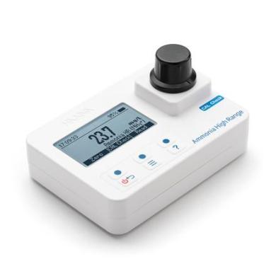
HANNA HI97733 Ammonia Photometer, up to 100.0 mg/L
Product Description
The HANNA HI97733 Ammonia Photometer, capable of measuring ammonia concentrations up to 100.0 mg/L, is a state-of-the-art device designed for precise and reliable assessments. With range adaptability between 1.0 and 100.0 mg/L (NH4+), the HI97733 ensures high-resolution measurements with an accuracy of ±0.5 mg/L ±5% of the reading at 25°C. Utilizing the Nessler method and adhering to the ASTM Manual of Water and Environmental Technology, D1426-92, it promises standardized, robust results. Equipped with two measuring cuvettes, plastic stoppers, caps, and batteries, this compact photometer is ready for immediate use. Its LED light source with a 420 nm narrow bandwidth filter, coupled with a silicon photocell detector, guarantees dependable quality and precision. The device holds up to 50 measurements for instant recall and features an auto-off function to conserve energy. With dimensions of 142.5 x 102.5 x 50.5 mm and a weight of 380 g, it offers portability without compromising functionality.
Item Stats
Product details
| Detail | Made in : Romania Serial No : 902400113111 |
About QuestPair
Our Mission
QuestPair is Europe's leading platform for scientific equipment, connecting researchers and organizations with verified suppliers of both new and pre-owned laboratory instruments in the biotech and material science industry. Our aim is to make the procurement of scientific instruments more efficient, cost-effective, and reliable, so that laboratories can focus on advancing science rather than searching equipment and negotiating deals.
Why Choose Us
Founded by scientists for scientists, we understand your challenges. Our AI-powered platform offers transparent pricing, verified quality, and expert support, ensuring you find the perfect equipment for your research needs.
Verified Quality
Every piece of equipment undergoes thorough verification by our expert team, ensuring reliability and performance.
Cost Efficiency
Access both new and premium pre-owned equipment, saving up to 40% without compromising on quality.
Expert Support
Our dedicated team provides personalized guidance throughout your equipment procurement journey.
Ready to Transform Your Research?
Join thousands of biotech scientists who trust QuestPair for their equipment needs.
What customers think about QuestPair
Brilliant service. Everything arrived and was exactly as expected
Jon Welburn
Great customer service! Got me great options for the equipment I was looking for and in a timely manner.
Pamela
Space Lab Technologies, LLCHarm is very responsive to help me find the right equipment. The product I received is in a good condition.
Ph.D. Hsin-Wen Liang
Northeastern UniversityPrice on Request
In Stock
Get a quote within one business day
Verified equipment
Trusted warranties & returns
Safe payment and fast delivery
Didn't find what you're looking for?
Our sales team specializes in sourcing custom and hard-to-find products to meet your exact specifications. Submit a request for a tailored quote.
Frequently Asked Questions
Is this equipment new or refurbished?
How long does shipping take?
What about warranty and returns?
Why request a quote?
Need help choosing the right tool?
- Accurate policy information specific to your chosen product
- Clear understanding of warranty coverage and terms
- Detailed return policy explanation
- Transparent shipping options and costs
Customer Service
Here to help you with: Product Inquiries, Shipping & Support, Technical Support, Business Inquiries and Press.
We are available to assist you Mon-Fri, 10am - 5pm CET.
